07. Process Flow Visualization
이 단계에서 확인할 내용
| Item | Description |
|---|---|
| Purpose | 전기적 결과를 해석하기 전에 공정 구조가 의도대로 형성됐는지 검증 |
| Method | 각 주요 SProcess 단계 직후 TDR 저장 |
| Output | 13개 checkpoint와 최종 대칭 구조 |
| Source | tdr_checkpoints.cmd |
TDR Command
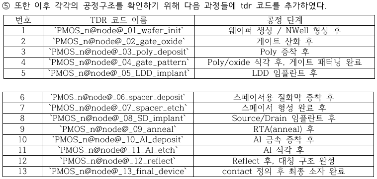
Figure. 공정 단계별 TDR 저장에 사용한 command.
struct tdr=PMOS_n@node@_01_wafer_init !Gas !interfaces
...
struct tdr=PMOS_n@node@_13_final_device !Gas !interfaces
Thirteen Checkpoints
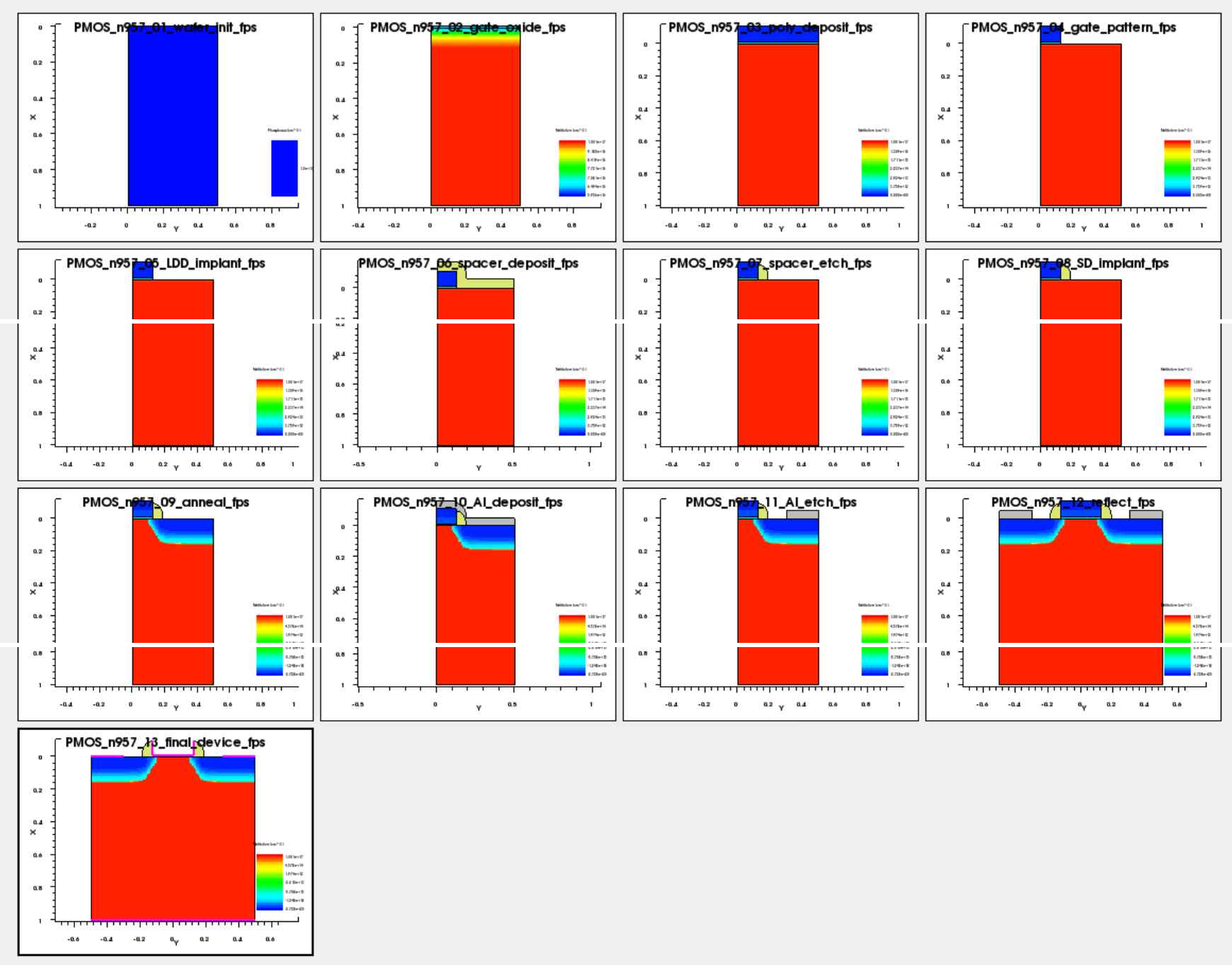
Figure. wafer initialization부터 final device까지의 13단계 구조.
| Step | TDR Name | Structure Check |
|---|---|---|
| 1 | 01_wafer_init |
NWell initialization |
| 2 | 02_gate_oxide |
gate oxide |
| 3 | 03_poly_deposit |
poly deposition |
| 4 | 04_gate_pattern |
gate patterning |
| 5 | 05_LDD_implant |
p-type LDD |
| 6 | 06_spacer_deposit |
nitride deposition |
| 7 | 07_spacer_etch |
sidewall spacer |
| 8 | 08_SD_implant |
p+ Source/Drain |
| 9 | 09_anneal |
activation and diffusion |
| 10 | 10_Al_deposit |
Al deposition |
| 11 | 11_Al_etch |
Al patterning |
| 12 | 12_reflect |
symmetric full structure |
| 13 | 13_final_device |
contact-defined final device |
Final Structure
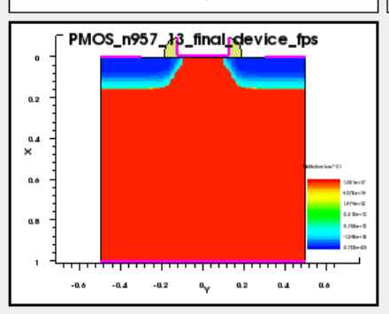
Figure. 최종 contact와 대칭 구조가 완성된 pMOS 단면.
Why Structural Verification Was Necessary
전기적 결과만 보면 다음 오류를 구분하기 어렵습니다.
- gate oxide 또는 poly pattern 형성 오류
- LDD와 Source/Drain 위치 오류
- spacer 조건 변경에 따른 과식각 또는 잔류
- anneal 이후 junction diffusion 변화
- reflect/contact 이후 최종 구조 완성 여부
TDR checkpoint는 각 split 결과가 구조 변화와 일치하는지 확인하는 근거로 사용했습니다.
Next: Method 1 Numerical Optimization
Summary:
Thirteen TDR checkpoints were used to verify the physical process sequence before interpreting electrical optimization results.