01 · OVERVIEW
프로젝트 개요
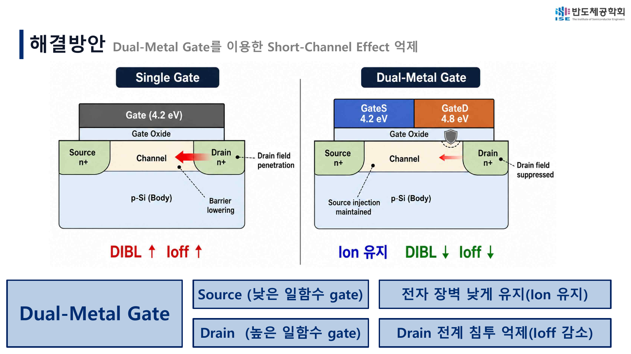
본 연구는 source 측에 낮은 work function을, drain 측에 높은 work function을 적용한 lateral Dual-Metal Gate 구조가 미세 MOSFET의 short-channel effect와 leakage에 미치는 상대적 영향을 확인한 feasibility study입니다.
생산 가능한 절대 최적 공정을 주장하기보다, 세 gate length에서 같은 방향의 효과가 반복되는지 검증하고 공정 조건, gate leakage, High-K stack과 gate-ratio 변화까지 단계적으로 확장했습니다.
This conference-presented study examines lateral work-function splitting in a 2D Sentaurus TCAD test vehicle and follows the research process from scaling and parameter screening to gate-leakage mitigation and gate-ratio analysis.
02 · RESEARCH QUESTION
연구 질문과 가설
Source-side low-WF gate는 carrier injection을 유지하고, drain-side high-WF gate는 drain field penetration과 barrier lowering을 억제하는 역할을 분리할 수 있는지 확인했습니다.
| Gate region | Work function | Intended role |
|---|---|---|
| GateS · source side | 4.2 eV | Ion 손실 제한 |
| GateD · drain side | 4.8 eV | Drain-side barrier lowering 억제 |
03 · IMPLEMENTATION
TCAD 공정 구현
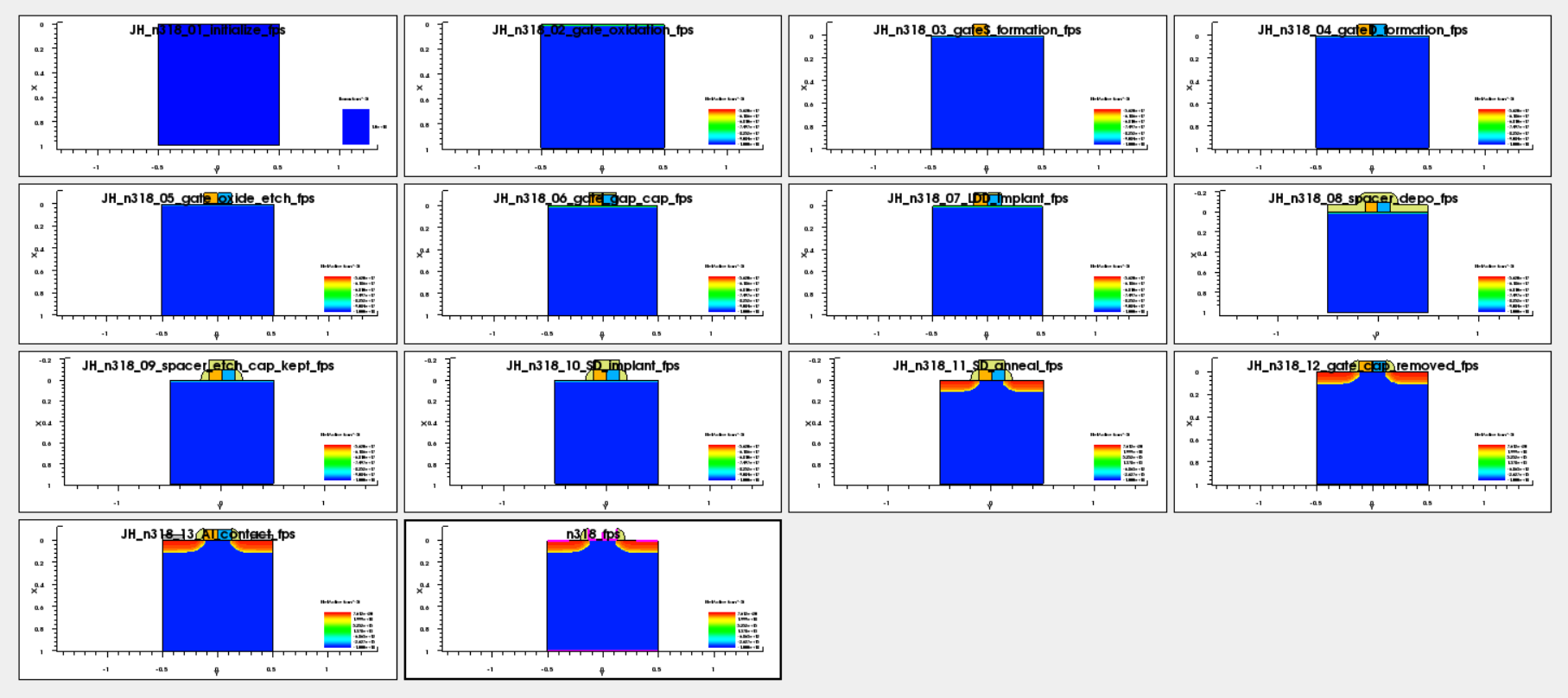
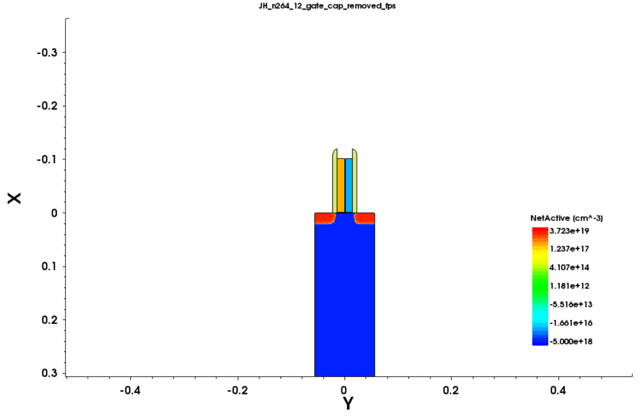
SProcess에서 GateS와 GateD를 서로 다른 material region으로 형성하고, 두 gate 사이에 작은 DMG gap을 두었습니다. Implant 중 gap을 통한 dopant 침투를 줄이기 위해 temporary nitride cap을 적용한 뒤 Source/Drain implant와 anneal 후 제거했습니다.
SDevice에서는 두 gate에 독립적인 work function을 지정하고 같은 gate voltage로 동시에 sweep했습니다. SVisual에서는 Vth, SS, gm, Ion, Ioff, Ion/Ioff와 DIBL을 자동 추출했습니다.
04 · SCALING & SCREENING
세 gate length의 검증과 조건 선정
각 scale에서 NWell, LDD dose/energy, Source/Drain dose/energy를 screening하고, Ion/Ioff–DIBL 분포와 SS·Ion을 함께 비교해 representative condition을 선정했습니다.
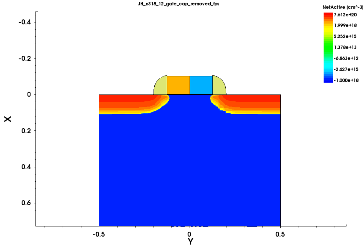
첫 효과 검증과 screening 방식 수립.
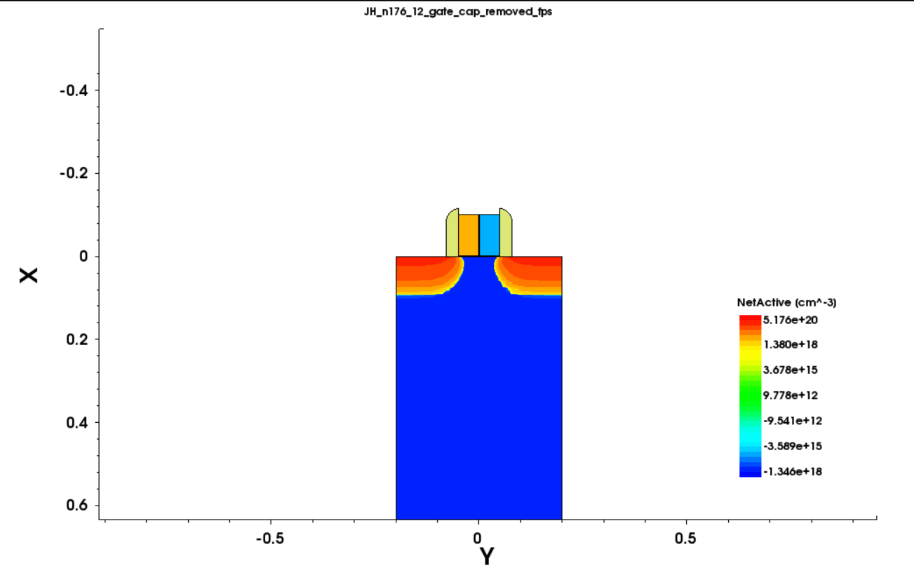
미세화 후 동일 방향 재검증.
구조 안정성 후 미세화 적용성 확인.
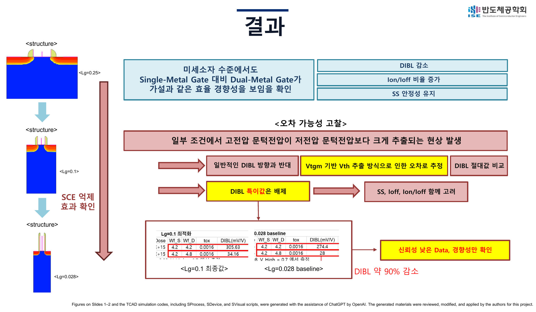
이 과정은 절대 최적화를 주장하는 작업이 아니라 여러 scale에서 DMG의 상대적 물리 효과를 확인하기 위한 parameter screening and comparative optimization입니다.
05 · LEAKAGE & HIGH-K
Gate leakage 문제와 High-K 개선
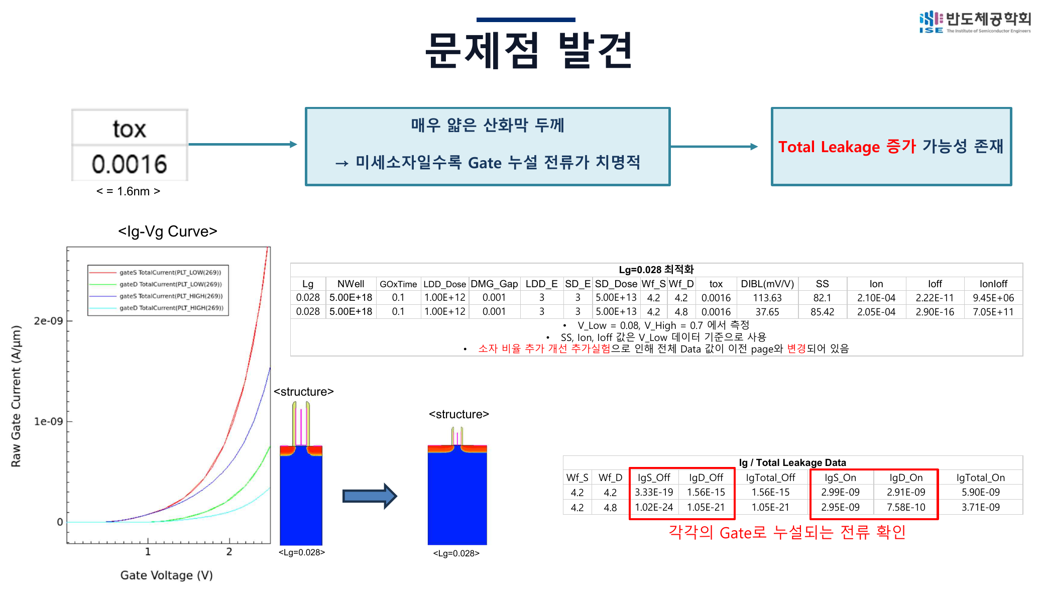
Lg = 0.028 μm에서 약 1.6 nm SiO₂를 사용할 경우 drain-current 기반 Ioff가 감소하더라도 on-state gate tunneling이 남는 것을 확인했습니다. 동일 EOT를 유지하면서 물리 두께를 늘리기 위해 SiO₂ interfacial layer/HfO₂ stack을 적용했습니다.
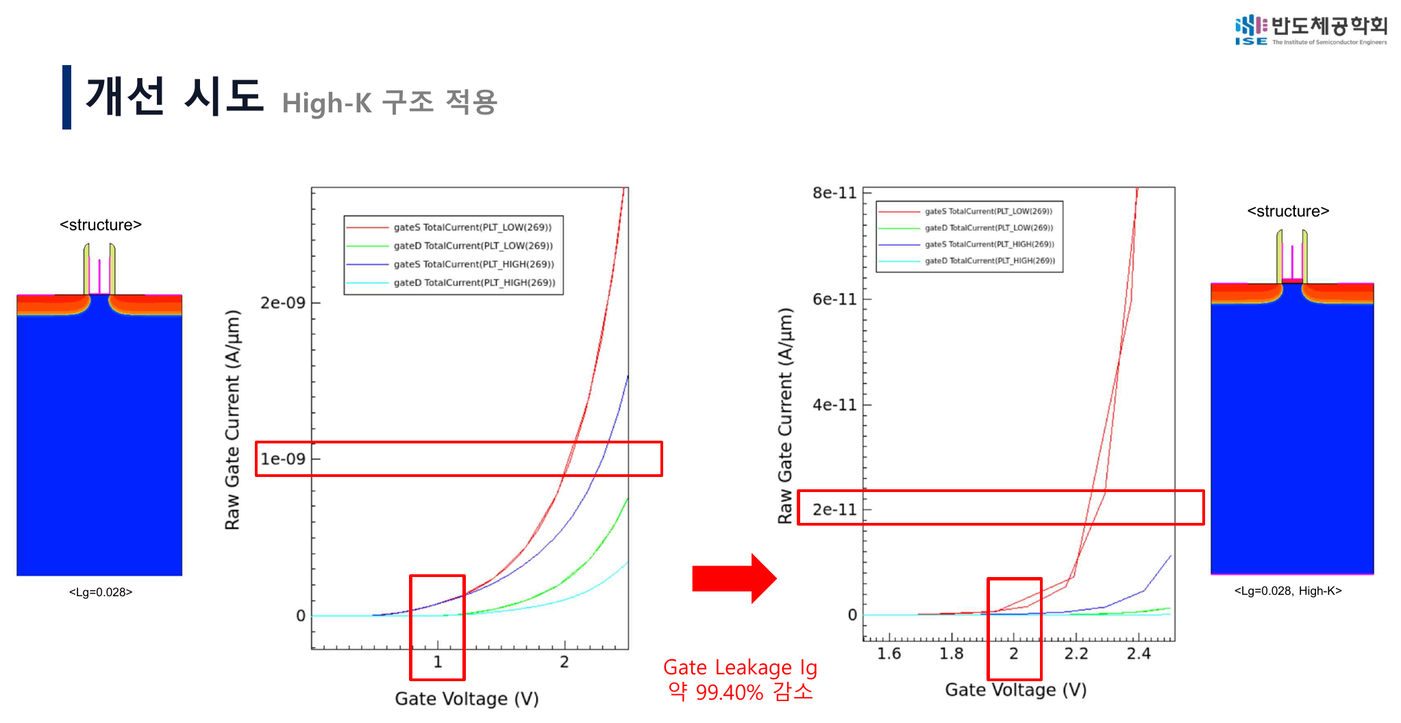
| Stack | EOT | Physical thickness | IgTotal On · High-Vd |
|---|---|---|---|
| SiO₂ | 1.6 nm | 1.6 nm | 1.8897e-9 A/μm |
| SiO₂ IL/HfO₂ | 1.5998 nm | 6.14 nm | 1.135e-11 A/μm |
대표 High-Vd 조건에서 IgTotal_On은 약 99.40% 감소했습니다. 이 수치는 calibrated absolute prediction이 아니라 동일 simulation framework 안에서 비교한 first-pass relative result입니다.
06 · GATE RATIO
GateS/GateD 비율 변화
총 gate region을 유지하면서 GateS:GateD를 6:4, 5:5, 4.5:5.5, 3.5:6.5로 변경했습니다. Drain-side high-WF 영역이 커질수록 Ioff, gate current와 SS는 개선되는 방향을 보였지만, GateS가 짧아지면서 Ion이 소폭 감소했고 DIBL은 비단조적으로 변했습니다.
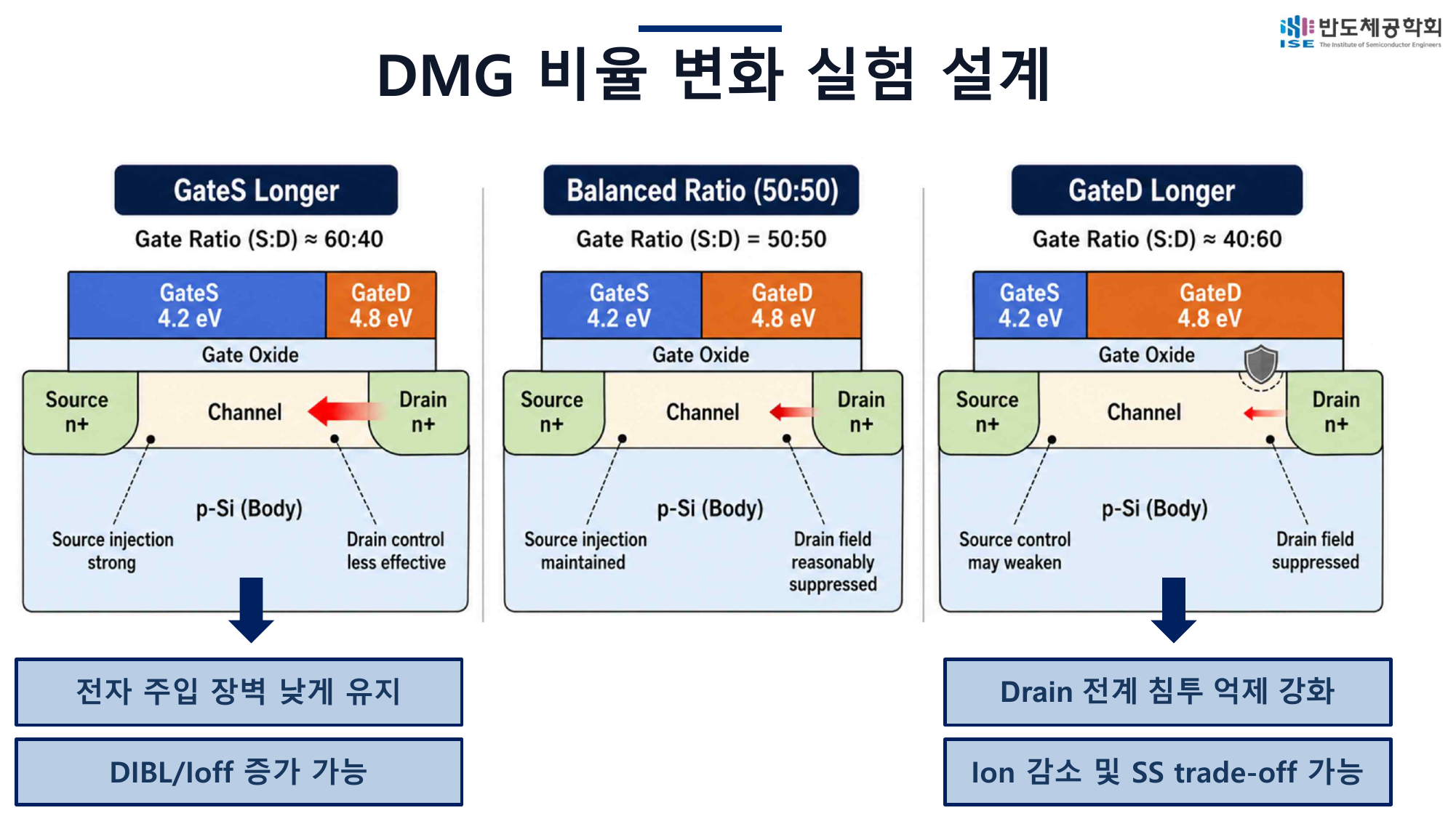
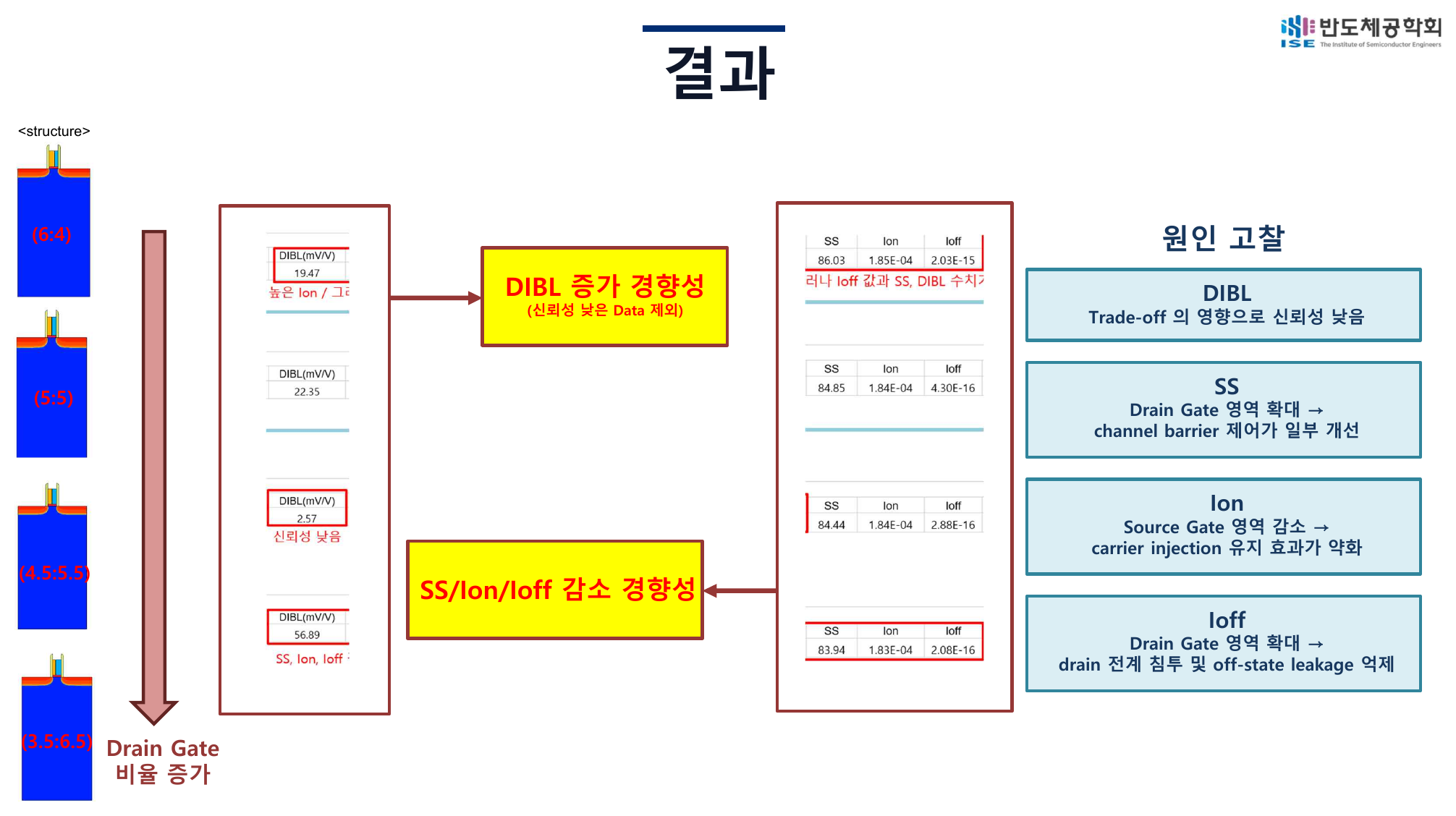
5:5는 모든 지표의 절대 최적점이 아니라 Ion 손실과 drain-side suppression을 함께 고려한 balanced reference condition입니다. 4.5:5.5의 매우 낮은 DIBL은 low-confidence data로 분류했습니다.
07 · CONCLUSION
핵심 결론과 연구 범위
- Source-side low WF와 drain-side high WF의 역할 분리 가능성을 확인했습니다.
- 세 gate length에서 Ion 일부 손실과 함께 Ioff와 Ion/Ioff가 개선되는 방향을 반복 확인했습니다.
- DIBL 특이값을 발견하고 SS, Ion, Ioff, Ion/Ioff를 함께 고려하는 신뢰성 정책을 도입했습니다.
- Thin-SiO₂ gate leakage를 추가 문제로 확인하고 High-K stack의 완화 가능성을 검토했습니다.
- Gate ratio는 하나의 절대 최적값이 아니라 source injection과 drain suppression의 trade-off 변수입니다.
본 결과는 2D planar TCAD test vehicle의 상대 비교입니다. 실제 GAA·CFET의 dual-WFM deposition, etch-back, alignment, metal filling과 variability를 실증한 결과가 아닙니다.
08 · RESOURCES